

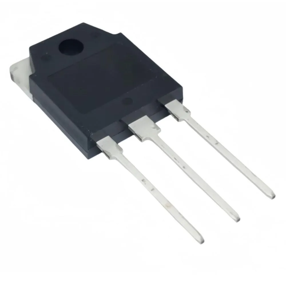

The BT40T60 is a power IGBT (Insulated Gate Bipolar Transistor) device in a TO-3P package (3-pin power module-style metal package). It is often used in switching power electronics applications such as inverters, UPSs, welding machines, motor drives, and power supplies. Its combination of MOSFET-like gate control with bipolar current conduction traits (i.e. IGBT) makes it suitable for medium-to-high voltage and moderate current switching.
One version of its datasheet is titled “Silicon FS Trench IGBT — BT40T60 ANFU”. The “FS” indicates “field-stop” structure, which helps improve performance by limiting tail currents and improving switching characteristics.
In many supplier listings, it is marketed as a 600 V, 40 A IGBT in TO-3P.
So the “BT40T60” is shorthand — many variants append “ANF,” “ANFU,” etc. — but they share the same core characteristics.
Key Features
Some of the standout features of the BT40T60 include:
| Feature | Description / Benefit |
|---|---|
| Voltage rating | It supports a collector-emitter voltage (V_CE) of up to 600 V (i.e. V_CES) |
| Current rating | Nominal current ratings are in the range of 40 A (continuous) in many listings |
| Field-stop/trench IGBT structure | This helps reduce switching and conduction losses compared to older IGBT designs |
| Low V_CE(sat) | The saturation voltage is relatively low (typical ~1.8 V at given currents) |
| High power dissipation | The device can handle significant power (e.g. ≈ 280 W in the datasheet) |
| Wide temperature range | The device supports elevated junction temperatures (up to ~150 °C) |
| TO-3P package | The TO-3P metal package assists in heat dissipation and robust mounting in high-power circuits |
Because of these features, the BT40T60 is a good choice in medium-voltage, medium-power switching applications where cost, reliability, and thermal management matter.
Technical Specifications
Below is a more detailed set of specifications (as available from datasheets / reference sources). Always consult the official manufacturer datasheet for final design work.
| Parameter | Typical / Rated Value |
|---|---|
| Collector-Emitter Voltage, V_CES (max) | 600 V |
| Gate-Emitter Voltage, V_GE (max) | ±20 V |
| Continuous Collector Current, I_C | ~40 A (in many commercial listings) |
| Power Dissipation, P_tot | ~280 W (at a specific case temperature) |
| V_CE(sat) | Typical ~1.8 V at 25 °C |
| Threshold Voltage, V_GE(th) | ~7 V (gate threshold) |
| Switching times (rise/fall) | Rise time (typical) ~50 ns |
| Output capacitance, C_oes (C<sub>oe</sub>) | ~170 pF (typical) |
| Maximum junction temperature, T_j(max) | 150 °C |
| Mounting / Package | TO-3P (3-pin power module) |
Notes / caveats:
-
The “40A” in many listings is a nominal current rating; the actual allowable current depends heavily on thermal management and ambient conditions.
-
The 280 W power dissipation is typically for a given case temperature (i.e. with good cooling).
-
The switching characteristics (rise/fall times, switching losses) depend on gate drive, stray inductances, and layout.
-
The device includes an anti-parallel diode (i.e. reverse conduction path) as is common with many power IGBTs.
Tips for Use & Design Guidelines
When using the BT40T60 (or any similar IGBT), here are some practical tips and best practices:
-
Thermal Management is Critical
-
Ensure a solid, low-thermal-resistance mounting to a heatsink or cold plate.
-
Use thermal interface materials (TIM) such as silicone pads or thermal paste to improve contact.
-
Monitor and limit junction temperature; operate well below T_j(max) under load.
-
-
Gate Drive Considerations
-
Use a proper gate driver capable of delivering sufficient current to charge and discharge the gate quickly (to reduce switching losses).
-
Limit gate voltage swing within ±20 V to avoid damage.
-
Consider using gate resistors to damp oscillations (due to parasitic inductances).
-
-
Minimize Parasitics
-
Keep leads/traces short and wide to reduce inductance and resistance.
-
Use proper decoupling capacitors close to the power device to supply transient currents.
-
Layout flow should minimize loop area of switching current paths.
-
-
Safe Operating Area (SOA) & Derating
-
Operate within the safe operating area especially in pulsed or transient conditions.
-
Derate current (i.e. use less than max rating) especially at elevated ambient temperatures.
-
-
Snubber / Protection Circuits
-
Use RC snubbers or clamp circuits to suppress voltage spikes due to inductive loads.
-
Consider transient voltage suppressors (TVS) or varistors across collector-emitter or across load for additional protection.
-
-
Switching Speed vs. Loss Tradeoff
-
Faster switching reduces conduction losses but increases switching losses and risk of overshoot.
-
Tune gate resistor and drive strength for an optimal compromise.
-
-
Check Safe Reverse Recovery Behavior
-
The anti-parallel diode and its reverse recovery should be considered in design, especially in bridge/inverter circuits.
-
-
Testing & Monitoring
-
During prototyping, monitor temperatures, voltage overshoots, and switching waveforms (with oscilloscope).
-
Use current limiting or soft-start during initial testing to avoid over-stressing the device.
-
-
Replacement / Interchangeability
-
When replacing or choosing substitutes, match voltage rating, current rating, package, and switching characteristics.
-
Check that V_CE(sat), gate charge, and thermal behavior are similar or better.
-
-
Reliability & Safety Margins
-
Always include margin in your design (e.g. design for 50–70% of maximum ratings).
-
Use proper fusing and protection in case of failure.
-

There are no reviews yet.