

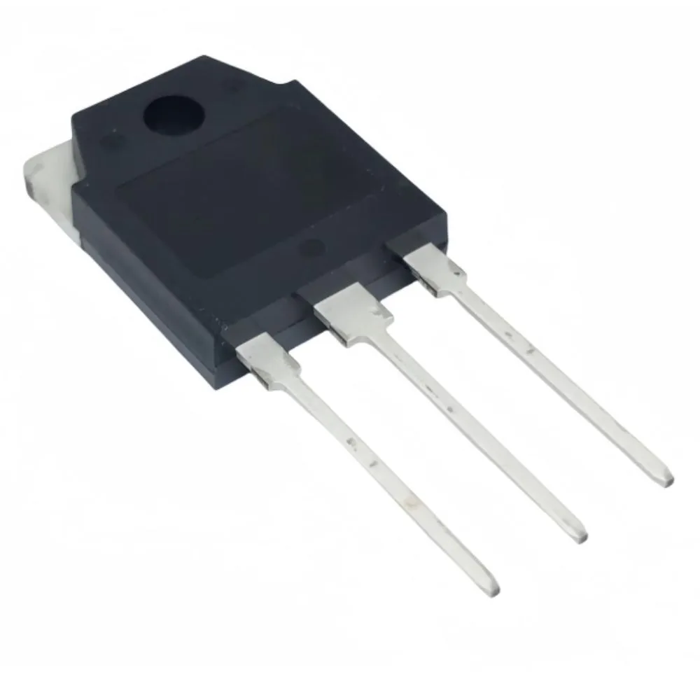
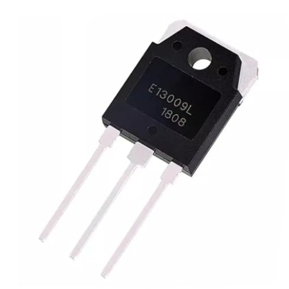
The BT60T60 (often seen as BT60T60ANFK) is a power IGBT (Insulated Gate Bipolar Transistor) packaged in the TO-3P (3-pin power module) form factor. It is designed for medium-voltage, medium-to-high current switching applications such as inverters, welding machines, UPS (uninterruptible power supplies), motor drives, and power supplies.
The “T60” suggests a 600 V class device. One source shows that the BT60T60ANFK supports a collector-emitter voltage of up to 600 V. The “60” in its designation often corresponds to a nominal current capability (or target class) under good thermal conditions.
One listing indicates the device has a maximum power dissipation (when case is held at 25 °C) of 403 W. The datasheet also describes it as a Field-Stop FS IGBT using trench technology, which is intended to reduce switching losses and improve performance.
Thus, the BT60T60 is meant for demanding switching tasks where both conduction and switching performance, along with thermal management, are critical.
Key Features
Some of the principal features and intended advantages of the BT60T60 include:
-
600 V blocking voltage: It supports a collector-emitter voltage up to 600 V in the off-state. High current capability: It can carry substantial collector current under favorable cooling (e.g. 60 A class).
-
High power dissipation: Up to ~403 W (at ideal case temperature) in continuous operation.
-
Low saturation voltage (V_CE(sat)): Typical ~1.85 V at 60 A and gate drive conditions. Trench & Field-Stop (FS) structure: To reduce switching losses and allow easier paralleling.
-
Robust junction temperature rating: Allowing operation up to ~150 °C.
-
TO-3P package: The metal-backed power module helps with heat sinking and provides mechanical/thermal robustness.
-
Anti-parallel diode capability: The device includes an internal diode path (or conduction path) for reverse current, which is common in IGBT modules.
Because of these, BT60T60 is suitable when you need both good conduction (low losses) and manageable switching behavior in medium-voltage domains.
Specifications (Typical & Maximum)
Below is a more detailed summary of the specifications of BT60T60ANFK (as gleaned from datasheet sources). Always refer to the official datasheet for precise and up-to-date values.
| Parameter | Value / Condition | Notes / Comments |
|---|---|---|
| Collector-Emitter Voltage, V_CES (max) | 600 V | Off-state breakdown rating |
| Gate-Emitter Voltage, V_GES (max) | ±20 V | Maximum safe gate voltage |
| Collector Current, I_C (continuous) | 60 A (at T_C = 100 °C) | At elevated case temperature |
| Collector Current, I_C (continuous, ideal cooling) | 120 A (at T_C = 25 °C) | Under ideal case cooling conditions |
| Pulsed Collector Current, I_CM | 180 A | For limited pulse durations |
| Power Dissipation, P_tot | 403 W (at T_C = 25 °C) | Maximum continuous dissipation under ideal case conditions |
| Zero gate leakage current, I_GES | ±250 nA | Gate leakage at ±20 V |
| Collector-Emitter Saturation Voltage, V_CE(sat) | Typical ~1.85 V (max ~2.4 V) at I_C = 60 A, V_GE = 15 V | Conduction drop characteristic |
| Threshold Voltage, V_GE(th) | ~4.0 to 7.0 V | Gate-turn-on threshold region |
| Input Capacitance, C_ies | ~3398 pF (V_CE = 30 V) | Gate-to-emitter + input capacitance |
| Output Capacitance, C_oes | ~224 pF | Collector-emitter capacitance in off state |
| Reverse Transfer Capacitance, C_res | ~44 pF | Feedback capacitance from collector to gate |
| Switching Delays / Times | t_d(on): 66 ns, t_r: 124 ns; t_d(off): ~152 ns, t_f: ~51 ns | Switching performance data (Rg = 10 Ω, V_GE = 15 V) |
| Switching Energy Losses (E_on / E_off) | E_on ≈ 4.79 mJ, E_off ≈ 1.39 mJ (for I_C = 60 A, V_CE = 400 V) | Losses under typical switching conditions |
| Reverse Diode Forward Voltage, V_F | ~1.3 to 1.6 V @ I_F = 30 A | Diode conduction characteristic |
| Reverse Recovery Time, t_rr | ~80 ns | Diode reverse recovery behavior |
| Reverse Recovery Current, I_rrm | ~6 A | Peak reverse recovery current |
| Junction Temperature, T_j (max) | 150 °C | Maximum operating temperature |
| Thermal Resistance, junction-to-case, R_θJC | ~0.31 °C/W (IGBT) | Thermal path rating from junction to metal mounting flange |
| Thermal resistance, junction-to-case (diode) | ~0.72 °C/W | For the anti-parallel diode path |
| Ambient thermal resistance, junction-to-ambient, R_θJA | ~40.1 °C/W | When mounted in free air (less ideal cooling) |
| Storage Temperature Range, T_stg | –55 to +150 °C | Safe storage conditions |
| Lead soldering temperature (max) | ~270 °C | At a specified distance from the device body |
| Package / Mechanical | TO-3P, metal flange, 3 leads | Dimensions and mechanical tolerances in datasheet |
Notes & caveats:
-
The “continuous current” ratings (60 A, 120 A) assume ideal case cooling (i.e. with good heatsinking, low thermal resistance). In practical circuit conditions with non-ideal cooling, the usable current will be lower to avoid overheating.
-
Switching times and losses depend strongly on gate drive strength, gate resistance, stray inductances, and the load conditions.
-
The power dissipation rating (403 W) is valid only when the case is held at 25 °C. As case/junction temperature rises, allowable dissipation must be derated significantly.
-
Safe Operating Area (SOA) considerations (especially under transients, pulses, or non-linear loads) must be respected; real-world stresses such as inductive kickbacks can exceed the device’s limits.
Practical Tips for Use & Design
To ensure reliable, efficient, and safe operation of a BT60T60 (or similar IGBT), consider the following guidance and design practices:
-
Thermal & Heatsinking Design
-
Use a high-quality heatsink or cold plate with low thermal resistance from the device’s backplate to ambient.
-
Use a good thermal interface material (e.g. solder, thermal grease, or thermal pad) to reduce thermal contact resistance.
-
Consider forced cooling (airflow or liquid) in high-power applications.
-
Always derate operation — e.g. aim to use only 50–70% of the device’s maximum ratings in typical design to leave margin for thermal and transient events.
-
-
Gate Drive Requirements
-
Use a gate driver capable of sourcing and sinking sufficient current to charge/discharge the gate capacitances quickly (to reduce switching losses).
-
Use a proper gate resistor (or damping network) to prevent ringing or oscillation due to parasitic inductances and capacitances.
-
Keep the gate-emitter voltage within allowed bounds (±20 V). Avoid overvoltage or undershoot.
-
Consider using a Miller clamp or active gate control to prevent unwanted turn-on via Miller effect during voltage transients.
-
-
Layout, Parasitics & Decoupling
-
Keep power loops (collector-emitter paths) as short and wide as possible to minimize stray inductance and resistance.
-
Place decoupling/bulk capacitors close to the device to supply rapid transient currents during switching.
-
Use snubber circuits (RC, RCD, or clamp diode networks) to limit voltage overshoots from inductive loads or wiring inductance.
-
Be cautious about layout symmetry if paralleling devices — ensure matched gate paths and current sharing.
-
-
Switching Speed vs Loss Tradeoffs
-
Faster switching reduces conduction losses but increases switching losses and overshoot stress — adjust gate resistor, gate drive strength to balance.
-
Monitor voltage and current waveforms (with a fast oscilloscope) during design/prototyping to identify overshoots, ringing, or unsafe conditions.
-
-
Protection & Safeguards
-
Use overcurrent protection (fuses, current limiting) to prevent device destruction under short-circuit conditions.
-
Incorporate voltage clamping (e.g. TVS diodes) to suppress transient spikes.
-
Use soft-start circuits to avoid abrupt inrush or stress at power-up.
-
Ensure safe operating area (SOA) margins; avoid pushing the device to its absolute limits continuously.
-
-
Parallel Operation (if needed)
-
If more current is required than one device can handle, ensure that devices are well matched (in V_CE(sat), switching behavior), and that thermal & gate drive symmetry is preserved.
-
Use small source resistors or emitter balancing to help even current sharing.
-
-
Testing & Monitoring
-
During initial testing, limit currents and voltages, and gradually increase towards target operating points while monitoring temperature, overshoots, and stability.
-
Use temperature sensors (e.g. thermocouples, thermal diodes, or IR) to monitor junction or case temperature in real time.
-
Monitor gate drive waveforms, switching edges, voltage overshoots, and current spikes using a high-speed oscilloscope and proper probing techniques.
-
-
Reliability & Safety Margins
-
Always operate with safety margin (e.g. not at 100% of rating).
-
Account for derating factors due to ambient temperature, thermal interface aging, and power cycling.
-
Ensure proper handling for static sensitivity (IGBTs are susceptible to ESD) — use ESD protection during assembly and handling.
-
-
Variant Verification
-
Confirm that the variant you have (e.g. ANFK, ANF, ANFU, etc.) matches the datasheet parameters you use, as there can be slight differences.
-
Cross-check pinouts, package thermal dimensions, and mechanical mounting.
-
There are no reviews yet.